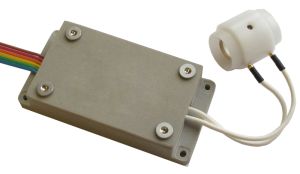
Pockels cell driver STA-PCD-1 has been designed for cavity dumping and Q-switching of solid-state lasers equipped with electrooptical Q-switches based on BBO or DKDP crystals. The modified version STA-PCD-2 provides unipolar output and may be used with Q-switches and modulators based on RTP, KTP, LITA, LNB crystals.
The device could also be used as a generator of nanosecond electrical pulses.
Further iterated STA-PCD-3 with integrated photoconductive switch allows the realization of a self-seeding mode that enhances SLM operation (contact Standa for more details).
| Model |
STA-PCD-1 |
STA-PCD-2 |
| Output voltage amplitude 1, 1a |
2800 ÷ 3800 V |
1400 - 1900 V |
| Output voltage pulse-to-pulse instability |
1 % |
| Max pulse current |
20 A |
| Max load capacitance |
20 pF |
| HV pulse rise time 2 |
2 ÷ 4 ns |
| HV pulse duration (factory-set) 3 |
0.5 ÷ 1 μs |
| HV pulse fall time |
3 ÷ 6 μs |
| Max HV pulse repetition rate |
2 kHz |
| Trigger voltage (input impedance is 200 Ohms) |
3 ÷ 8 V (+5 V) |
| Output pulse delay vs. trigger pulse 4 |
15 ÷ 30 ns |
| HV pulse jitter |
< 200 ps |
| External powering requirements: |
| Low voltage DC supply |
+5 to +7.5 V |
| Low voltage DC supply current |
| at a repetition rate of 100 Hz |
180 mA |
| at a repetition rate of 1 kHz |
260 mA |
| at a repetition rate of 2 kHz |
340 mA |
| Operating temperature range |
10 ÷ 40 °C |
| Dimensions |
30 x 50 x 9 mm |
| Mounting hole pattern (Ø 3.2 mm) |
24 x 44 mm |
| Wiring diagram |
View |
1 is set from the built-in potentiometer or remotely
1a max. output voltage amplitude could be achieved while driver is supplied with +7.5 V voltage
2 depends on the load inductance and output voltage amplitude.
3 is set by manufacturer.
4 Delay depends on the trigger pulse. The higher trigger amplitude the shorter delay.
| Model |
STA-PCD-3A |
STA-PCD-3M |
| Output voltage amplitude 1 |
1180 ÷ 1400 V |
400 - 1500 V |
| Closing voltage ( HV2 ), controlled by CTRL2 voltage |
0 ÷ 1000 V |
| Max load capacitance |
15 pF |
| HV pulse rise time 2 |
1.4 ÷ 1.8 ns |
4 ÷ 6 ns |
| HV pulse duration (factory-set) 3 |
0.5 ÷ 0.7 μs |
0.5 ÷ 1.0 μs |
| HV pulse fall time |
1.5 ÷ 3 μs |
| Max HV pulse repetition rate |
5 kHz |
40 kHz |
| Trigger voltage (input impedance is 200 Ohms) |
+5 V (TTL) |
| Output pulse delay vs. trigger pulse 4 |
15 ÷ 30 ns |
| HV pulse jitter5 |
< 80 ps |
< 200 ps |
| Control voltages HV1, and HV26 (CTRL1, CTRL2) |
0 ÷ 2.5 V |
| External powering requirements: |
| Low voltage DC supply |
+7.5 V |
+7.5 V
+15 V |
| Low voltage DC supply current |
| Operating temperature range |
+15 to 50 °C |
| Dimensions |
39.5 x 95 x 40.5 mm |
1 Depends on HV 1 supply. Max. output voltage amplitude could be achieved while HV1 = 1000 V
2 Depends on the load inductance and output voltage amplitude.
3 Set by manufacturer.
4 Delay depends on the trigger pulse quality
5 f trigger pulse rise time < 0.5 ns
6 HV1 = 400 * (CTRL1); HV2 = 400 * (CTRL2)
| Related products |
|
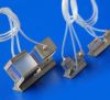
RTP EO Q-switch |
STA-PCD-1 packaged with BBO based Pockels cell | |


